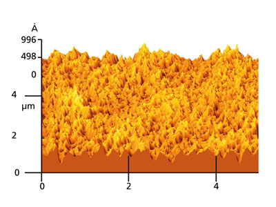
By using atomic force microscopy, it is possible to image the microstructure of surfaces down to the nanometer scale and, for example, to demonstrate the plasma-technological increase in the micro-roughness of plastics. Average roughness values can be calculated via image evaluation. Different modes provide not only the topography but also the material contrast.
Atomic force microscopy (AFM) and scanning tunneling microscopy (STM)
The principle
A very sharp tip with a tip radius of a few nanometers scans the surface to be examined line by line. A reflected laser beam aimed at a quadrant photodiode registers the deflection of the tip, and the signal is fed back to a piezo crystal. A computer as a topographic image records the motion of the piezo. The interaction force of the tip with the surface is kept constant (constant-force). In some cases (e.g. at atomic resolution) the height of the piezo crystal can also be kept constant (constant-height).
Measuring equipment/measuring possibilities
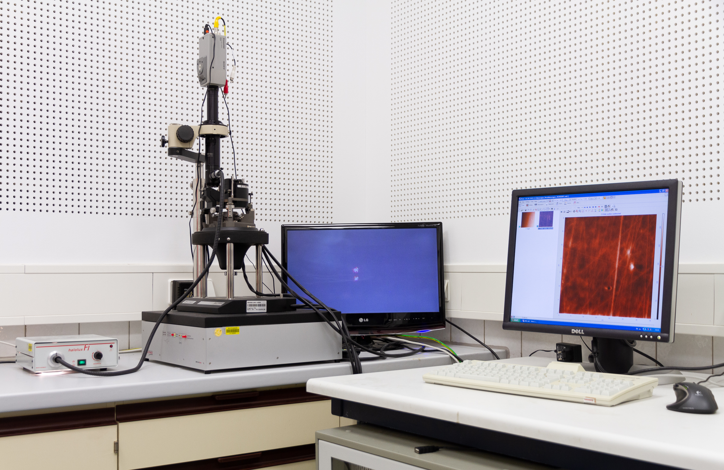
Solver Pro from NTMDT
Technical data
optical microscope for pre-adjustment of the sample measuring heads for:
- contact mode and non-contact mode with force modulation and phase shift measurement
- lateral force mode
- STM
- liquid measuring cell
- option for electrochemical measurements
- resolutions down to the atomic range
- max. scan size: 30 x 30 µm
- Topographies of surfaces from the microscopic to the atomic range can be displayed.
- Roughness can be determined easily.
- In contrast to the electron microscope, no sample pre-treatment and no vacuum are necessary.
- Layer thickness measurement on edges
- Friction and elasticity differences
Requirements for the test material
- Maximum specimen size 4 x 4 cm2 (ideally 1,5 x 1,5 cm2)
- Maximum roughness: 3 µm
 Fraunhofer Institute for Interfacial Engineering and Biotechnology IGB
