High-resolution scanning electron microscopy (FE-SEM) with electron- and X-ray-induced EDX analytics

© Fraunhofer IGB
GeminiSEM 500.

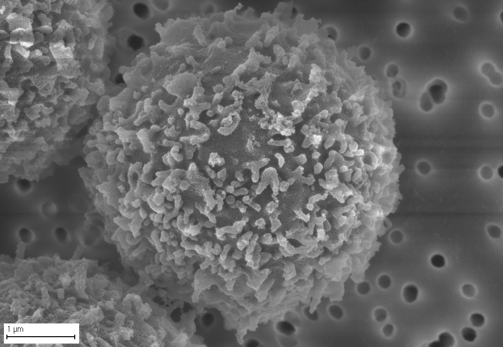
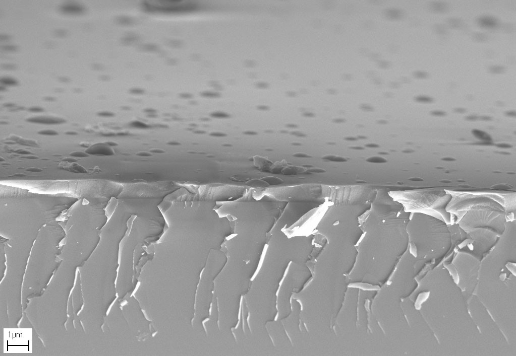
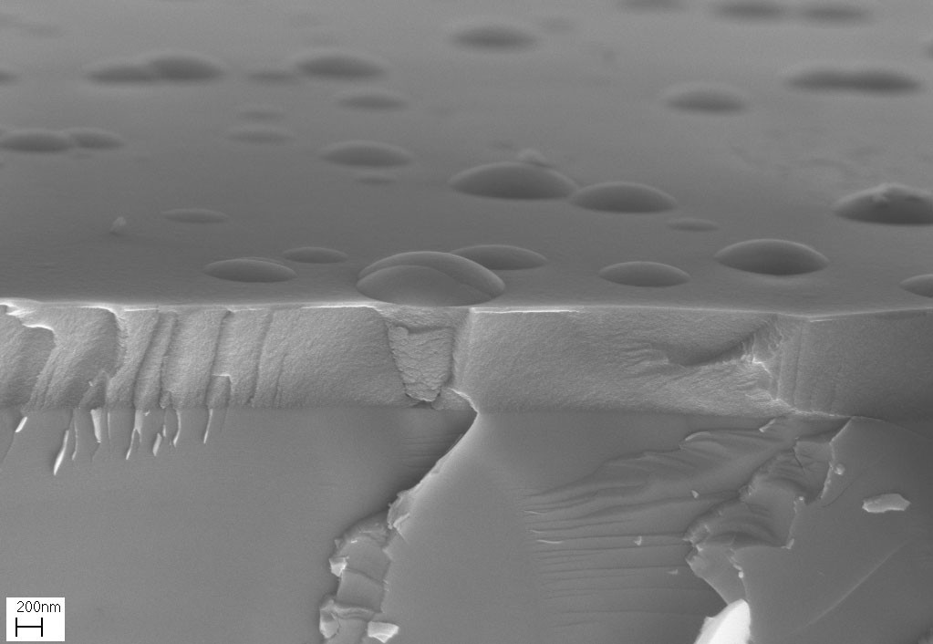
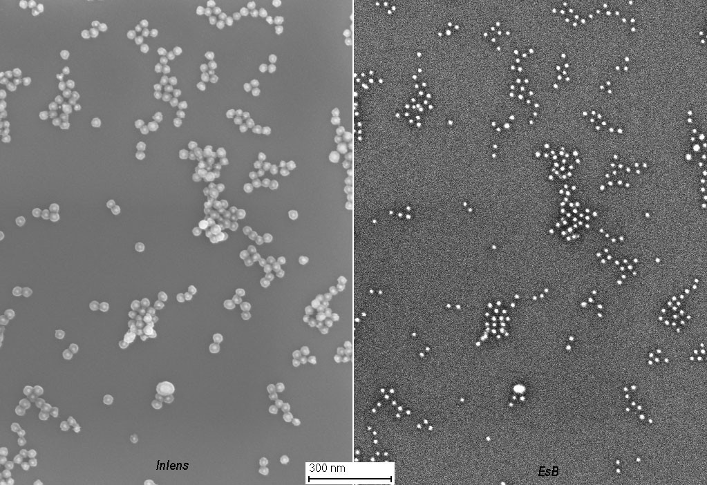
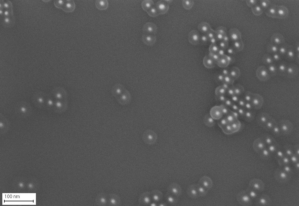
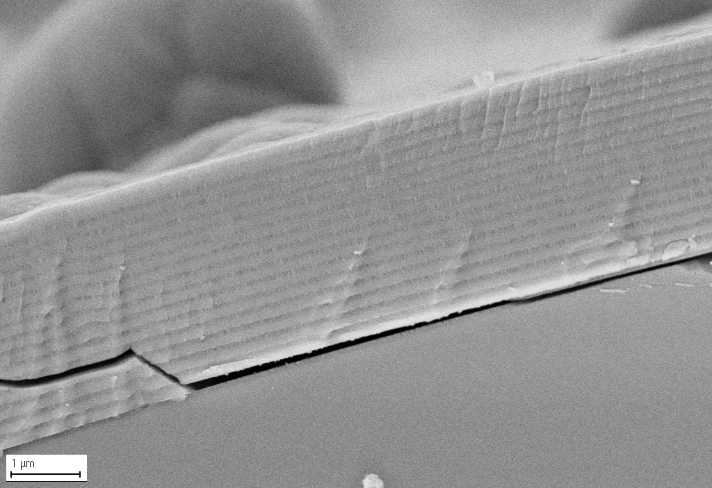
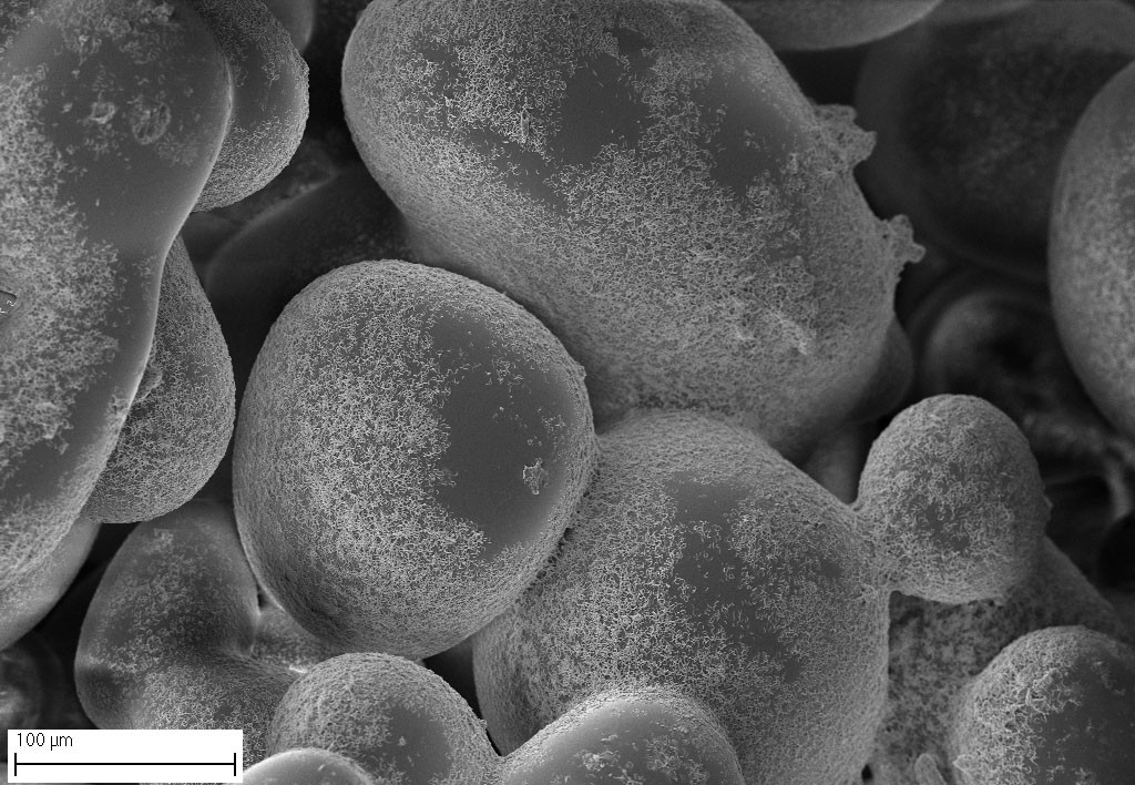
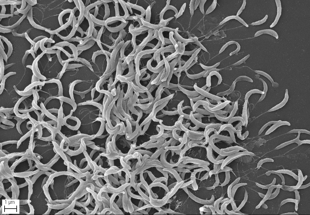
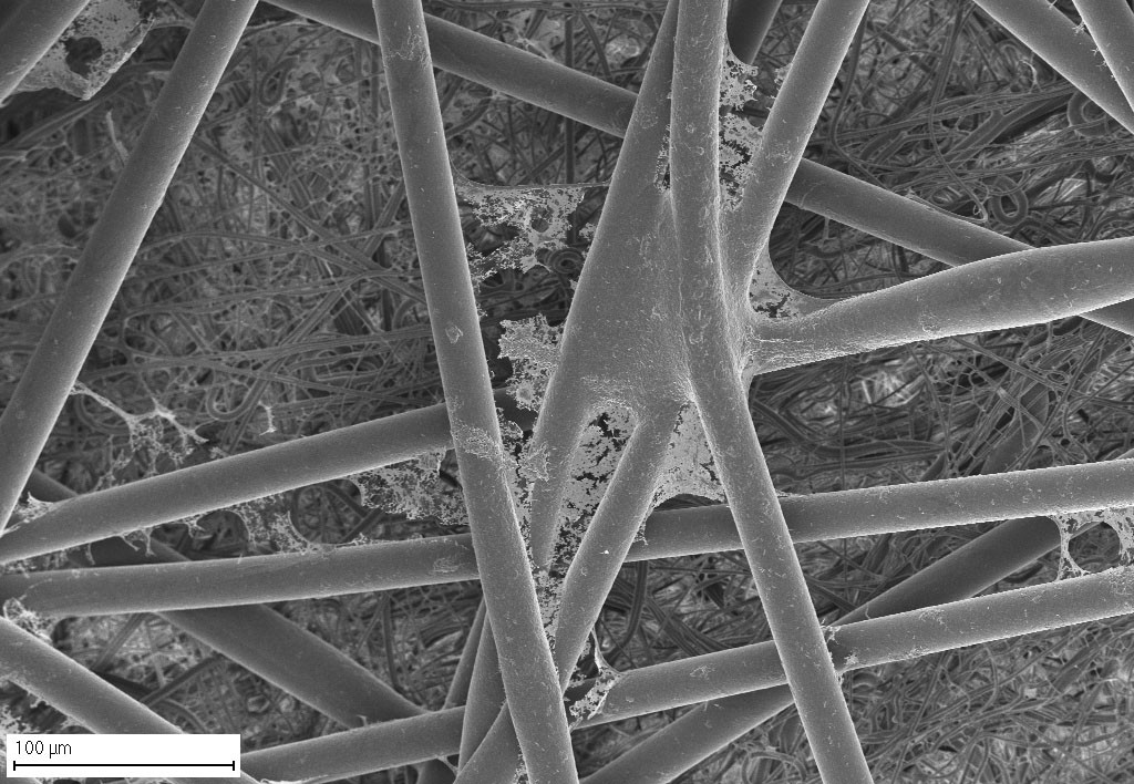
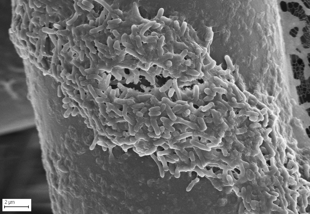
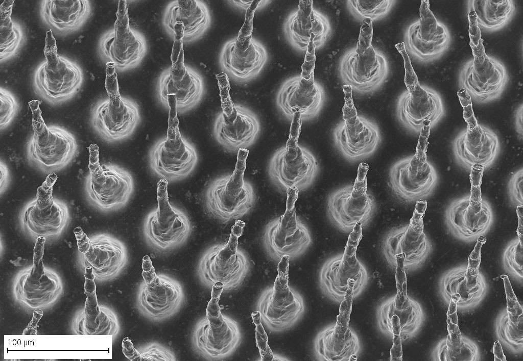
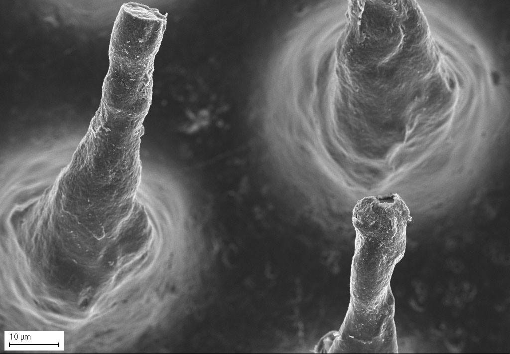
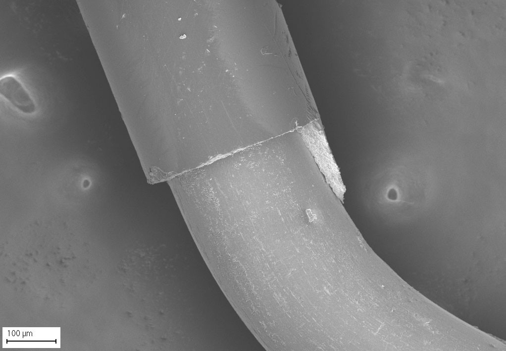
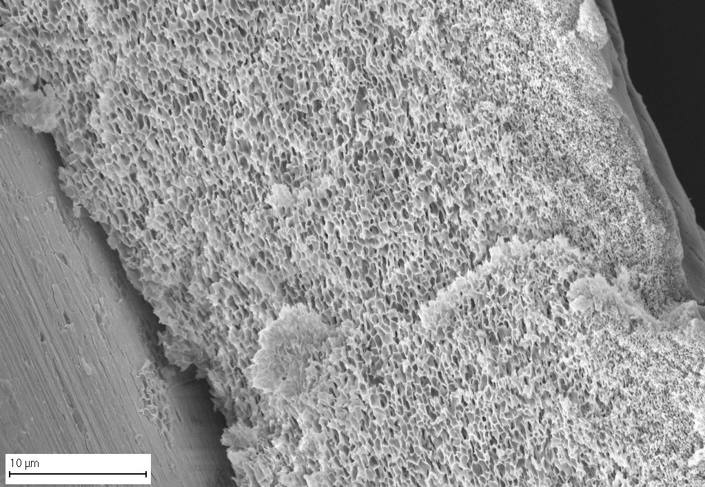
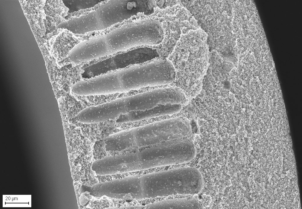
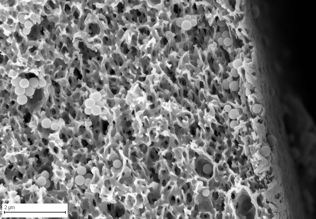
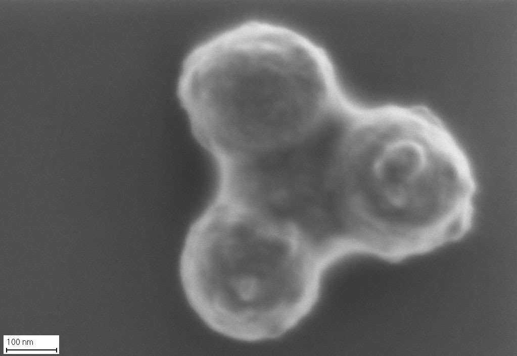
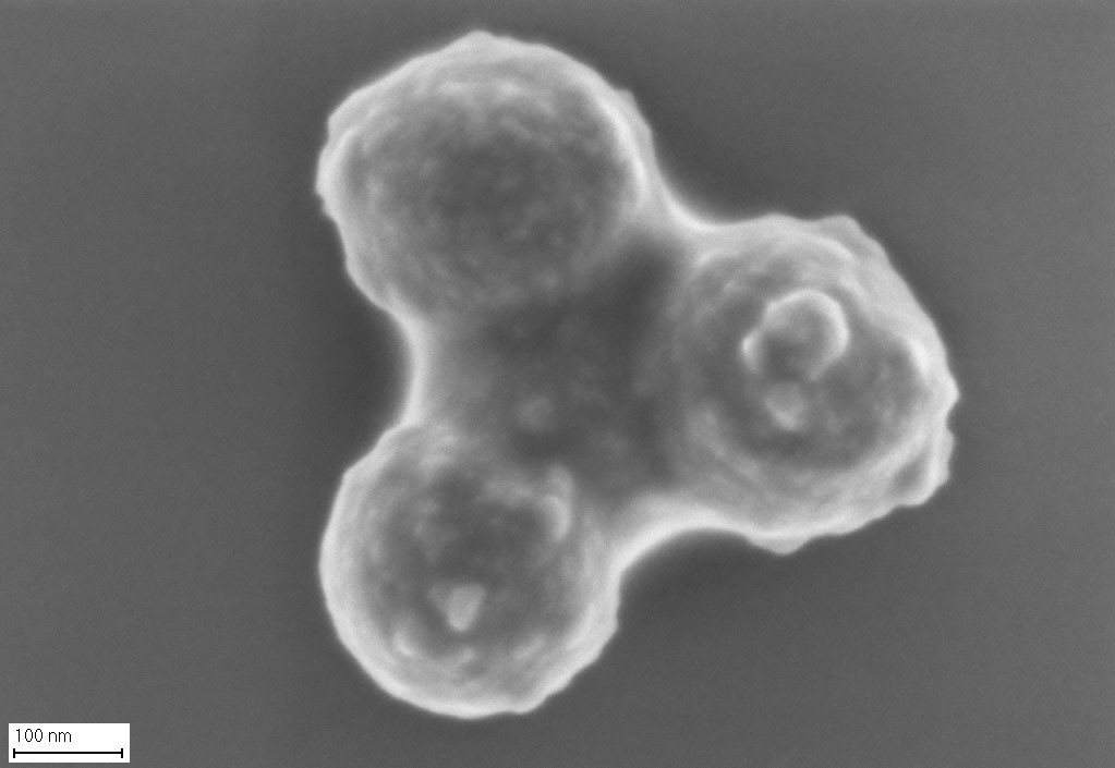
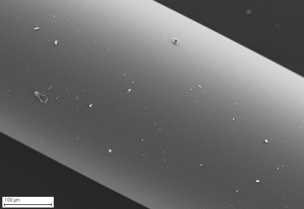
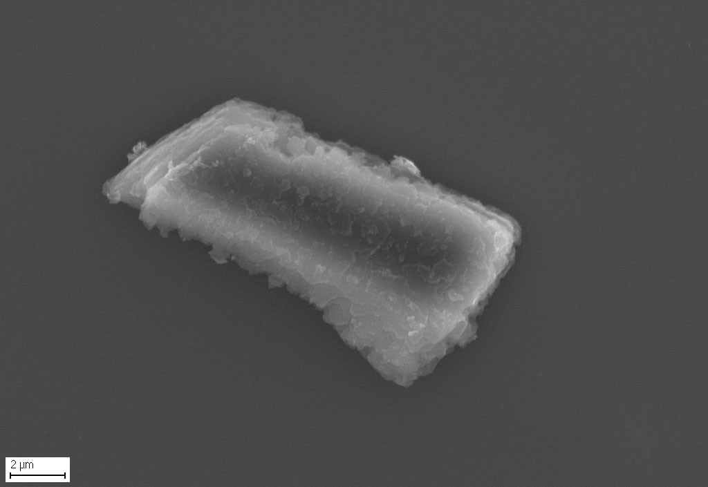
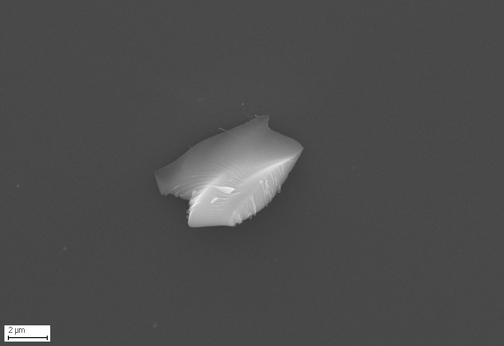
By means of scanning electron microscopy, the observation of surface shapes of spatially structured objects is possible over a large magnification range.

With suitable sample preparations, it is feasible to examine surfaces or fracture edges of almost all materials that have vacuum stability.

In interfacial, nanoparticle or membrane analysis, the analysis and visualization of structures in the range of a few nanometers to micrometers provides information and clues about pore and particle size, cracks and roughness, cavities or other special shapes.

The GeminiSEM500 (Fa. Zeiss SMT) available at Fraunhofer IGB is a field emission scanning electron microscope (FE SEM). Additionally, the microscope is suitable for the analysis of radiation-sensitive samples, non-conductive materials as well as to obtain near-surface information on the nature of the sample.

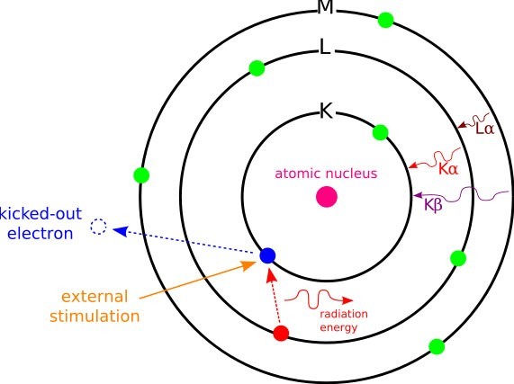
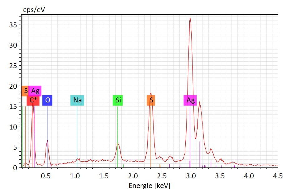
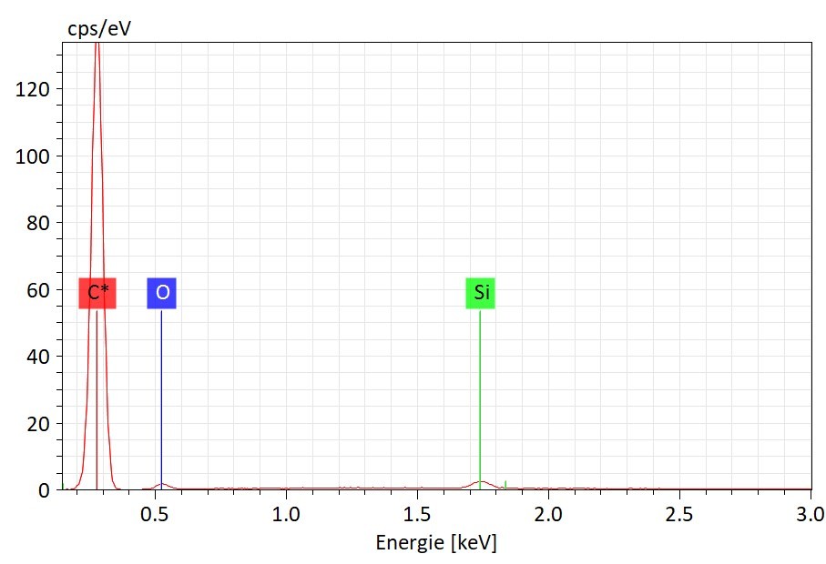
Interaction of the electron beam with the sample produces X-rays that provide information about the chemical elemental composition. Two EDX detectors (XFlash and FlatQuad Fa. Bruker Nano) are installed for this purpose. SEM imaging can be used to locate specific sample sites of interest and to detect even small elemental composition differences in the smallest volumes.

Principle and signals in a scanning electron microscope

Interaction volume and signals.

A primary electron beam is generated with the aid of an electrode cathode and acceleration towards the anode. The anode focuses as finely as possible by subsequent electromagnetic lenses onto the surface of the sample to be examined.

A thermal Schottky field emitter guarantees a high and stable beam current intensity. A cross over free electron optical column (beam booster) allows high-resolution imaging and signal acquisition in the low voltage range. High-resolution imaging of non-conductive materials is also possible with a so-called NanoVP device with variable pressure settings and under certain conditions and circumstances.

In the sample, secondary electrons (SE1 and SE2), backscattered electrons (BSE) and X-rays are generated in an interaction volume that depends on the acceleration voltage and the material composition. The energy of the X-rays depends on the atomic number of the emitting atom and is thus "characteristic" for the element in question. Appropriate detectors are able to register all of these signals. Topography, material and/or element contrasts can be mapped in this way.

Microanalysis system (EDX and micro-XRF)

Formation of characteristic X-ray quanta induced by incident electrons or X-rays.

The X-rays generated in the electron microscope by the interaction between the sample and the incident electrons can be used analytically by the additional extension of EDX detectors. Thus, the determination of the local chemical composition of the sample material on a surface imaged by the SEM is possible. Depending on the accelerating voltage and the sample matrix, a spatial resolution of about 1 µm and where appropriate even lower is practicable.

It is then possible to record spot measurements, line profiles or element distribution images.

By irradiating the sample material with a finely focusable X-ray source (XTrace Source, micro XRF), element-specific fluorescence radiation is excited. The analysis and detection of trace elements or heavier elements in the sub mm range is feasible.

Specimen requirements and applications

The sample material must be in solid form, it should be vacuum compatible (low vapor pressure, negligible gas emission) and it should be insensitive to electron beams.

The sample size should ideally be less than 1 cm in height and approximately 1 cm² in area (can be cut to size). Investigations, also of larger sample dimensions, are possible with consultation and, if necessary, agreed pre-preparations.

Possible applications and areas of use

  • Topography and morphology of technical materials and functional surfaces, e.g. visualization of deposits, microbial growth, (particulate) contamination, etc.
  • Cross-section or fracture edge view of polymeric and inorganic materials
  • Representation and determination of layer thicknesses and layer structures
  • Representation and determination of pore size/density or cavities of membranes
  • Representation and determination of particle and structure sizes of nanomaterials
  • Representation and (element) identification of material defects/inclusions

Application examples: Nanotechnology, engineering materials, membranes, functional surfaces, polymers and inorganic materials, microorganisms.

 Surface structure of human white blood cells (WBC)

© Fraunhofer IGB
Poor sample preparation, no cell separation, washed out surface structure.
© Fraunhofer IGB
Successful preparation, finest structures visible on the surface.

Fracture preparation of a plasma deposition

A low-pressure plasma was used to create a layer deposition on a smooth substrate surface. A uniform thickness can be seen, but also significant defect areas.

© Fraunhofer IGB
© Fraunhofer IGB

Core-shell Nanoparticles

© Fraunhofer IGB
Left half of image: InLens SE1 signal. | Right half of image: EsB detector, low-energy backscattered electrons (BSE).
© Fraunhofer IGB
Mixed signal acquisition, image with SE1 and BSE, the boundary between envelope and core is clearly visible.

Cross-sectional view of a multiple layer stack deposition

Alternating layers, each about 80 nm thick, with different material compositions are visible. A total of 32 layer stacks.


© Fraunhofer IGB
© Fraunhofer IGB

Biofilm deposits on spherical glass supports

© Fraunhofer IGB
© Fraunhofer IGB

Dense growth of microorganisms on coarse-mesh polymeric nonwoven fabric


© Fraunhofer IGB
© Fraunhofer IGB
© Fraunhofer IGB

3D structuring of a polymeric material

Regular "hat shape" pressed into foil. The image shows a raised structure with a high aspect ratio.


© Fraunhofer IGB
© Fraunhofer IGB

Spray-dried nano- and microparticles

Micro- and nanoparticles produced from phosphate buffer by spray drying.

© Fraunhofer IGB
Overview image.
© Fraunhofer IGB
Detailed view, adsorbed salt crystals on the particle surface are visible.

Membrane coating on metal wire

A membrane coating was applied to a thin metal wire (Ø 0.3 mm).

© Fraunhofer IGB
Overview image.
© Fraunhofer IGB
Detail, cross-sectional view of the membrane layer at a broken site.

Polymeric mixed-matrix hollow fiber membrane in cross-section

© Fraunhofer IGB
The porous structure of the membrane shows finger-like macrovoids to the inner surface.
© Fraunhofer IGB
Particles smaller than 1 µm embedded in the structure are recognizable.

High-resolution imaging of the surface structure of nanoparticles

Nanoparticles approximately 300 nm in size were prepared by emulsion polymerization. The sample was not sputtered.

© Fraunhofer IGB
The particle surface appears blurred and out of focus.
© Fraunhofer IGB
The image acquisition was performed with significantly lower KV, a fine structure is now visible.

Glass capillary with particulate impurities

© Fraunhofer IGB
Preparation of the thin (Ø approx. 0.4mm) glass capillaries on SEM specimen holders.
© Fraunhofer IGB
SEM overview view, the particulate impurities in the size of a few µm are visible.

Subsequent images and spectra

SEM detail view and EDX spectra of particles. The EDX spectra give an indication of the different elemental composition of the particles.

© Fraunhofer IGB
Particle 1
© Fraunhofer IGB
Particle 2
© Fraunhofer IGB
Particle 3
© Fraunhofer IGB
Particle 1
© Fraunhofer IGB
Particle 2
© Fraunhofer IGB
Particle 3